PC54CVIP (VER. 1.0) Motherboard Settings and Configuration
SEANIX TECHNOLOGY, INC.
PC54CVIP (VER. 1.0)
Processor | Pentium |
Processor Speed | 75/90/100MHz |
Chip Set | OPTI |
Max. Onboard DRAM | 128MB |
Cache | 256/512KB |
BIOS | Award |
Dimensions | 330mm x 218mm |
I/O Options | 32-bit VESA local bus slots (2), 32-bit PCI slots (4) |
NPU Options | None |
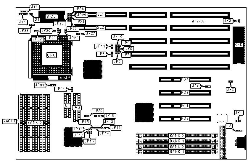
CONNECTIONS | |||
Purpose | Location | Purpose | Location |
External battery | J2 | 32-bit PCI slots | PC1 - PC4 |
Power LED & keylock | J17 | Reset switch | S1 |
Speaker | J18 | 32-bit VESA local bus slots | SL1 & SL2 |
USER CONFIGURABLE SETTINGS | |||
Function | Jumper | Position | |
» | Factory configured - do not alter | JP1 | pins 2 & 3 closed |
» | Factory configured - do not alter | JP2 | Open |
» | Fast VL-BUS disabled | JP3 | Open |
Fast VL-BUS enabled | JP3 | Closed | |
» | Flash memory voltage select 5v | JP4 | pins 1 & 2 closed |
Flash memory voltage select 12v | JP4 | pins 2 & 3 closed | |
» | Factory configured - do not alter | JP7 | Open |
» | Factory configured - do not alter | JP8 | Open |
» | Factory configured - do not alter | JP12 | Open |
» | Back to back I/O delay select fast | JP15 | Closed |
Back to back I/O delay select slow | JP15 | Open | |
» | Factory configured - do not alter | JP16 | pins 1 & 2 closed |
» | Factory configured - do not alter | JP17 | Closed |
» | LDEV sample select end of second T2 | JP18 | Closed |
LDEV sample select end of first T2 | JP18 | Open | |
» | Factory configured - do not alter | JP19 | Open |
» | L1 cache type select always invalidated | JP20 | pins 1 & 2 closed |
L1 cache type select invalidated on write only | JP20 | pins 2 & 3 closed | |
» | Factory configured - do not alter | JP21 | pins 2 & 3 closed |
» | Factory configured - do not alter | JP22 | Open |
» | Factory configured - do not alter | JP23 | Open |
» | Factory configured - do not alter | JP24 | Open |
» | Factory configured - do not alter | JP25 | Closed |
» | Factory configured - do not alter | JP26 | Open |
» | Factory configured - do not alter | JP27 | Open |
» | Factory configured - do not alter | JP31 | pins 1 & 2 closed |
» | Memory mapping I/O at top of memory | JP32 | pins 1 & 2 closed |
128MB installed running UNIX | JP32 | pins 2 & 3 closed | |
» | CPU bus/core ratio enabled | JP33 | pins 1 & 2 closed |
CPU bus/core ratio disabled | JP33 | pins 2 & 3 closed | |
DRAM CONFIGURATION | ||
Size | Bank 0 | Bank 1 |
2MB | (2) 256K x 36 | NONE |
4MB | (2) 512K x 36 | NONE |
4MB | (2) 256K x 36 | (2) 256K x 36 |
6MB | (2) 256K x 36 | (2) 512K x 36 |
8MB | (2) 1M x 36 | NONE |
8MB | (2) 512K x 36 | (2) 512K x 36 |
10MB | (2) 256K x 36 | (2) 1M x 36 |
12MB | (2) 512K x 36 | (2) 1M x 36 |
16MB | (2) 2M x 36 | NONE |
16MB | (2) 1M x 36 | (2) 1M x 36 |
18MB | (2) 256K x 36 | (2) 2M x 36 |
DRAM CONFIGURATION (CON’T) | ||
Size | Bank 0 | Bank 1 |
20MB | (2) 512K x 36 | (2) 2M x 36 |
24MB | (2) 1M x 36 | (2) 2M x 36 |
32MB | (2) 4M x 36 | NONE |
32MB | (2) 2M x 36 | (2) 2M x 36 |
34MB | (2) 256K x 36 | (2) 4M x 36 |
36MB | (2) 512K x 36 | (2) 4M x 36 |
40MB | (2) 1M x 36 | (2) 4M x 36 |
48MB | (2) 2M x 36 | (2) 4M x 36 |
64MB | (2) 8M x 36 | NONE |
64MB | (2) 4M x 36 | (2) 4M x 36 |
66MB | (2) 256K x 36 | (2) 8M x 36 |
68MB | (2) 512K x 36 | (2) 8M x 36 |
72MB | (2) 1M x 36 | (2) 8M x 36 |
80MB | (2) 2M x 36 | (2) 8M x 36 |
96MB | (2) 4M x 36 | (2) 8M x 36 |
128MB | (2) 8M x 36 | (2) 8M x 36 |
CACHE CONFIGURATION | |||
Size | Bank 0 | TAG | DIRTY (U1) |
256KB | (8) 32K x 8 | (1) 32K x 8 | (1) 8K x 8 |
512KB | (8) 64K x 8 | (1) 64K x 8 | (1) 8K x 8 |
CACHE JUMPER CONFIGURATION | |||
Size | JP28 | JP29 | JP30 |
256KB | Open | Closed | Closed |
512KB | Closed | Closed | Closed |
CPU SPEED CONFIGURATION (MK1432 CLOCK) | |||||
Speed | JP5 | JP6 | JP9 | JP10 | JP11 |
75MHz | 1 & 2 | Open | Closed | Open | 2 & 3 |
90MHz | 1 & 2 | Open | Open | Open | 2 & 3 |
100MHz | 1 & 2 | Closed | Open | Open | 2 & 3 |
Note: Pins designated should be in the closed position. | |||||
CPU SPEED CONFIGURATION (9154A-42 CLOCK) | |||||
Speed | JP5 | JP6 | JP9 | JP10 | JP11 |
75MHz | 1 & 2 | Open | Open | Open | 2 & 3 |
90MHz | 1 & 2 | Closed | Closed | Open | 2 & 3 |
100MHz | 1 & 2 | Closed | Open | Open | 2 & 3 |
Note: Pins designated should be in the closed position. | |||||
LCLK CONFIGURATION | ||
LCLK | JP13 | JP14 |
2 | Open | Open |
3 | Closed | Open |
4 | Open | Closed |
5 | Closed | Closed |
My Books

