P5-PCI-VL Motherboard Settings and Configuration
SEANIX TECHNOLOGY, INC.
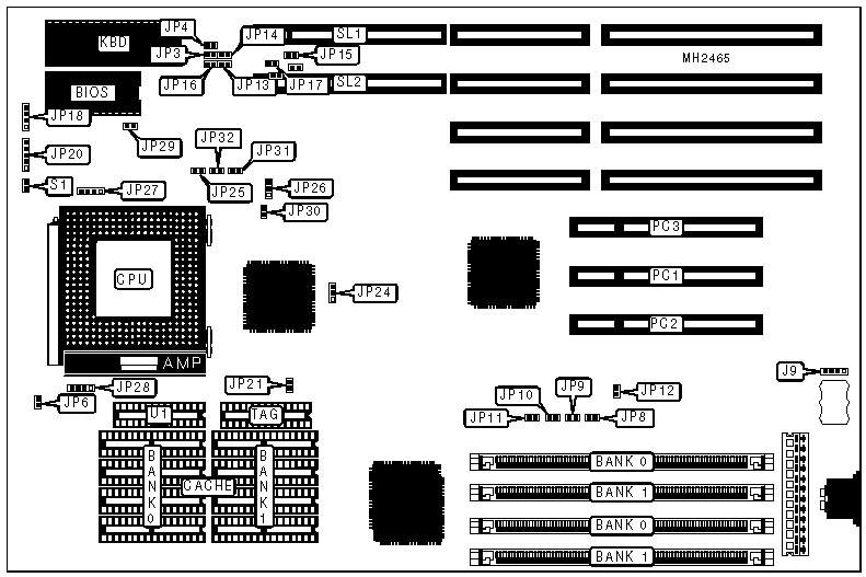
P5-PCI-VL
Processor | Pentium |
Processor Speed | 60/66MHz |
Chip Set | OPTI |
Max. Onboard DRAM | 128MB |
Cache | 256/512/1024KB |
BIOS | Award |
Dimensions | 330mm x 218mm |
I/O Options | 32-bit VESA local bus slots (2), 32-bit PCI slots (3) |
NPU Options | None |
CONNECTIONS | |||
Purpose | Location | Purpose | Location |
External battery | J9 | Chassis fan power | JP28 |
Speaker | JP18 | 32-bit PCI slots | PC1 - PC3 |
Power LED & keylock | JP20 | Reset switch | S1 |
Secondary CPU fan | JP27 | 32-bit VESA local bus slots | SL1 & SL2 |
USER CONFIGURABLE SETTINGS | |||
Function | Jumper | Position | |
» | Factory configured - do not alter | JP3 | N/A |
» | Factory configured - do not alter | JP4 | N/A |
» | Factory configured - do not alter | JP8 | N/A |
» | Factory configured - do not alter | JP9 | Closed |
» | Factory configured - do not alter | JP10 | N/A |
» | Factory configured - do not alter | JP11 | N/A |
» | Factory configured - do not alter | JP12 | N/A |
» | Factory configured - do not alter | JP13 | N/A |
» | Factory configured - do not alter | JP14 | N/A |
» | Factory configured - do not alter | JP15 | N/A |
» | Factory configured - do not alter | JP16 | N/A |
» | Factory configured - do not alter | JP17 | N/A |
» | Factory configured - do not alter | JP24 | N/A |
» | Flash BIOS write protect enabled | JP29 | Open |
Flash BIOS write protect disabled | JP29 | Closed | |
DRAM CONFIGURATION | ||
Size | Bank 0 | Bank 1 |
2MB | (2) 256K x 36 | NONE |
4MB | (2) 512K x 36 | NONE |
4MB | (2) 256K x 36 | (2) 256K x 36 |
6MB | (2) 256K x 36 | (2) 512K x 36 |
8MB | (2) 1M x 36 | NONE |
8MB | (2) 512K x 36 | (2) 512K x 36 |
10MB | (2) 256K x 36 | (2) 1M x 36 |
12MB | (2) 512K x 36 | (2) 1M x 36 |
16MB | (2) 2M x 36 | NONE |
16MB | (2) 1M x 36 | (2) 1M x 36 |
18MB | (2) 256K x 36 | (2) 2M x 36 |
20MB | (2) 512K x 36 | (2) 2M x 36 |
24MB | (2) 1M x 36 | (2) 2M x 36 |
32MB | (2) 4M x 36 | NONE |
32MB | (2) 2M x 36 | (2) 2M x 36 |
34MB | (2) 256K x 36 | (2) 4M x 36 |
36MB | (2) 512K x 36 | (2) 4M x 36 |
40MB | (2) 1M x 36 | (2) 4M x 36 |
48MB | (2) 2M x 36 | (2) 4M x 36 |
64MB | (2) 8M x 36 | NONE |
64MB | (2) 4M x 36 | (2) 4M x 36 |
66MB | (2) 256K x 36 | (2) 8M x 36 |
68MB | (2) 512K x 36 | (2) 8M x 36 |
72MB | (2) 1M x 36 | (2) 8M x 36 |
80MB | (2) 2M x 36 | (2) 8M x 36 |
96MB | (2) 4M x 36 | (2) 8M x 36 |
128MB | (2) 8M x 36 | (2) 8M x 36 |
CACHE CONFIGURATION | ||||
Size | Bank 0 | Bank 1 | TAG | DIRTY BIT (U1) |
256KB | (4) 32K x 8 | (4) 32K x 8 | (1) 32K x 8 | (1) 32K x 8 |
512KB | (4) 64K x 8 | (4) 64K x 8 | (1) 32K x 8 | (1) 32K x 8 |
1MB | (4) 128K x 8 | (4) 128K x 8 | (1) 32K x 8 | (1) 32K x 8 |
CACHE JUMPER CONFIGURATION | ||
Size | JP6 | JP21 |
256KB | Open | Open |
512KB | Open | Closed |
1MB | Closed | Closed |
CPU FREQUENCY CONFIGURATION (AV9107-4) | |||||
Speed | JP25 | JP26 | JP30 | JP31 | JP32 |
50MHz | Closed | pins 2 & 3 closed | Closed | Open | Closed |
60MHz | Open | pins 1 & 2 closed | Closed | Open | Open |
66MHz | Closed | pins 2 & 3 closed | Open | Closed | Closed |
CPU FREQUENCY CONFIGURATION (CH9007E) | |||||
Speed | JP25 | JP26 | JP30 | JP31 | JP32 |
50MHz | Open | pins 2 & 3 closed | Open | Open | Closed |
60MHz | Open | pins 2 & 3 closed | Open | Closed | Open |
66MHz | Open | pins 2 & 3 closed | Closed | Closed | Open |
My Books

