ADVANCED/ML Motherboard Settings and Configuration
YOUNG MICRO SYSTEMS, INC.
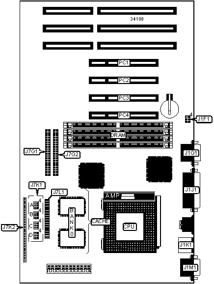
ADVANCED/ML
Processor | Pentium |
Processor Speed | 75/90/100/120/133/150/166MHz |
Chip Set | Intel |
Video Chip Set | None |
Maximum Onboard Memory | 128MB (EDO supported) |
Maximum Video Memory | None |
Cache | 256/512KB |
BIOS | Unidentified |
Dimensions | 304mm x 178mm |
I/O Options | 32-bit PCI slots (4), floppy drive interface, green PC connector, IDE interfaces (2), parallel port, PS/2 mouse port, serial ports (2), IR connector |
NPU Options | None |
CONNECTIONS | |||
Purpose | Location | Purpose | Location |
Serial port 1 | J1G1 | Reset switch | J7K2 pins 4 & 5 |
Parallel port | J1J1 | Power LED & keylock | J7K2 pins 6 - 10 |
PS/2 mouse port | J1K1 | IDE interface LED | J7K2 pins 11 - 14 |
Serial port 2 | J1M1 | Green PC connector | J7K2 pins 15 - 19 |
IDE interface | J7G1 | IR connector | J7K2 pins 20 - 25 |
IDE interface | J7G2 | Speaker | J7K2 pins 26 - 29 |
Floppy drive interface | J7L1 | 32-bit PCI slots | PC1 - PC4 |
Chassis fan power | J7K2 pins 1 - 3 | ||
USER CONFIGURABLE SETTINGS | |||
Function | Label | Position | |
» | Factory configured - do not alter | J1F1 | Unidentified |
» | Password normal operation | J7K1A | Pins 1 & 2 closed |
Password clear | J7K1A | Pins 2 & 3 closed | |
» | CMOS memory normal operation | J7K1A | Pins 4 & 5 closed |
CMOS memory clear | J7K1A | Pins 5 & 6 closed | |
» | Setup access enabled | J7K1B | Pins 1 & 2 closed |
Setup access disabled | J7K1B | Pins 2 & 3 closed | |
DRAM CONFIGURATION | ||
Size | Bank 0 | Bank 1 |
8MB | (2) 1M x 36 | None |
16MB | (2) 2M x 36 | None |
16MB | (2) 1M x 36 | (2) 1M x 36 |
24MB | (2) 2M x 36 | (2) 1M x 36 |
32MB | (2) 4M x 36 | None |
32MB | (2) 2M x 36 | (2) 2M x 36 |
40MB | (2) 4M x 36 | (2) 1M x 36 |
48MB | (2) 4M x 36 | (2) 2M x 36 |
64MB | (2) 8M x 36 | None |
64MB | (2) 4M x 36 | (2) 4M x 36 |
72MB | (2) 8M x 36 | (2) 1M x 36 |
80MB | (2) 8M x 36 | (2) 2M x 36 |
96MB | (2) 8M x 36 | (2) 4M x 36 |
128MB | (2) 8M x 36 | (2) 8M x 36 |
Note: Board accepts EDO memory. Board also accepts x 32 SIMMs. The location of banks 0 & 1 are unidentified. | ||
CACHE CONFIGURATION | |
Size | Bank 0 |
256KB | (2) 32K x 32 |
512KB | (2) 64K x 32 |
CPU SPEED SELECTION | ||||
CPU speed | Clock speed | Multiplier | J7K1C | J7K1D |
75MHz | 50MHz | 1.5x | 2 & 3, 5 & 6 | 1 & 2, 4 & 5 |
90MHz | 60MHz | 1.5x | 2 & 3, 4 & 5 | 1 & 2, 4 & 5 |
100MHz | 66MHz | 1.5x | 1 & 2, 5 & 6 | 1 & 2, 4 & 5 |
120MHz | 60MHz | 2x | 2 & 3, 4 & 5 | 2 & 3, 4 & 5 |
133MHz | 66MHz | 2x | 1 & 2, 5 & 6 | 2 & 3, 4 & 5 |
150MHz | 60MHz | 2.5x | 2 & 3, 4 & 5 | 2 & 3, 5 & 6 |
166MHz | 66MHz | 2.5x | 1 & 2, 5 & 6 | 2 & 3, 5 & 6 |
Note: Pins designated should be in the closed position. | ||||
CPU TYPE SELECTION | ||
Type | J7K1B | |
OVD | Pins 5 & 6 closed | |
| » | VRE | Pins 4 & 5 closed |
My Books

