SYSTEM BOARD D1005 Motherboard Settings and Configuration
SIEMENS-NIXDORF INFORMATIONSSYSTEME AG
SYSTEM BOARD D1005
Device Type | Mainboard |
Processor | Pentium II |
Processor Speed | 233/266/300MHz |
Chip Set | Unidentified |
Video Chip Set | None |
Maximum Onboard Memory | 256MB (EDO supported) |
Maximum Video Memory | None |
Cache | 256/512KB (located on Pentium II CPU) |
BIOS | Unidentified |
Dimensions | 305mm x 244mm |
I/O Options | 32-bit PCI slots (4), floppy drive interface, game/MIDI port, green PC connector, IDE interfaces (2), parallel port, PS/2 mouse port, serial ports (2), IR connector, USB connectors (2), line in, line out, microphone in, wavetable connector, audio in – CD-ROM, telephony connectors (2) |
NPU Options | None |
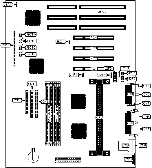
CONNECTIONS | |||
Purpose | Location | Purpose | Location |
Game/MIDI port | CN1 | Telephony connector | J2F3 |
Microphone in | CN2 | Audio in – CD-ROM | J2F6 |
Line in | CN3 | Line in (auxiliary) | J3F1 |
Line out | CN4 | Chassis fan power | J4F1 |
Serial port 2 | CN5 | Security connector | J6C1 |
Serial port 1 | CN6 | Chassis fan power | J9A1 |
Parallel port | CN7 | Soft off power supply | J9D1/pins 1 & 2 |
USB connector 1 | CN8 | Green PC connector | J9D1/pins 3 & 4 |
USB connector 2 | CN9 | IR connector | J9D1/pins 6 - 11 |
PS/2 mouse port | CN10 | IDE interface LED | J9D1/pins 13 - 16 |
IDE interface 2 | CN11 | Power LED | J9D1/pins 18 - 20 |
IDE interface 1 | CN12 | Reset switch | J9D1/pins 22 & 23 |
Floppy drive interface | CN13 | Speaker | J9D1/pins 24 - 27 |
Telephony connector | J2F1 | 32-bit PCI slots | PC1 – PC4 |
Wavetable connector | J2F2 | ||
USER CONFIGURABLE SETTINGS | |||
Function | Label | Position | |
» | Flash BIOS normal operation | J9C1A | Pins 5 & 6 closed |
Flash BIOS recovery mode | J9C1A | Pins 4 & 5 closed | |
» | CMOS memory normal operation | J9C1C | Pins 5 & 6 closed |
CMOS memory clear | J9C1C | Pins 4 & 5 closed | |
» | Setup access enabled | J9C1D | Pins 5 & 6 closed |
Setup access disabled | J9C1D | Pins 4 & 5 closed | |
SIMM CONFIGURATION | ||
Size | Bank 0 | Bank 1 |
8MB | (2) 1M x 36 | None |
16MB | (2) 2M x 36 | None |
16MB | (2) 1M x 36 | (2) 1M x 36 |
24MB | (2) 2M x 36 | (2) 1M x 36 |
32MB | (2) 4M x 36 | None |
32MB | (2) 2M x 36 | (2) 2M x 36 |
40MB | (2) 4M x 36 | (2) 1M x 36 |
48MB | (2) 4M x 36 | (2) 2M x 36 |
64MB | (2) 8M x 36 | None |
64MB | (2) 4M x 36 | (2) 4M x 36 |
SIMM CONFIGURATION (CON’T) | ||
Size | Bank 0 | Bank 1 |
72MB | (2) 8M x 36 | (2) 1M x 36 |
80MB | (2) 8M x 36 | (2) 2M x 36 |
96MB | (2) 8M x 36 | (2) 4M x 36 |
128MB | (2) 8M x 36 | (2) 8M x 36 |
128MB | (2) 16M x 36 | None |
136MB | (2) 16M x 36 | (2) 1M x 36 |
144MB | (2) 16M x 36 | (2) 2M x 36 |
160MB | (2) 16M x 36 | (2) 4M x 36 |
192MB | (2) 16M x 36 | (2) 8M x 36 |
256MB | (2) 16M x 36 | (2) 16M x 36 |
Note: Board accepts EDO memory. | ||
CACHE CONFIGURATION |
Note: 256KB/512KB cache is located on the Pentium II CPU. |
CPU SPEED SELECTION | |||||
CPU speed | Clock speed | Multiplier | J9C1A | J9C1B | J9C1C |
233MHz | 66MHz | 3.5x | 2 & 3 | 2 & 3, 5 & 6 | 2 & 3 |
266MHz | 66MHz | 4x | 1 & 2 | 1 & 2, 4 & 5 | 2 & 3 |
300MHz | 66MHz | 4.5x | 1 & 2 | 2 & 3, 4 & 5 | 2 & 3 |
Note: Pins designated should be in the closed position. | |||||
My Books

