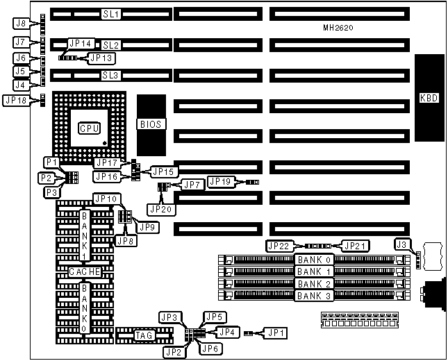
CK-491K Motherboard Settings and Configuration
CHICONY, INC.
CK-491K
Processor | CX486S/80486SX/80487SX/CX486DX/80486DX/CX486DX2/80486DX2/ 80486DX4/Pentium Overdrive |
Processor Speed | 20/25/33/40/50(internal)/50/66(internal)/75(internal)/100(internal)MHz |
Chip Set | Unidentified |
Max. Onboard DRAM | 64MB |
Cache | 32/64/128/256KB |
BIOS | AMI |
Dimensions | 330mm x 218mm |
I/O Options | 32-bit VESA local bus slots (3) |
NPU Options | None |
CONNECTIONS | |||
Purpose | Location | Purpose | Location |
External battery | J3 | Speaker | J7 |
Reset switch | J4 | Power LED & keylock | J8 |
Turbo switch | J5 | 32-bit VESA local bus slots | SL1 - SL3 |
Turbo LED | J6 | ||
USER CONFIGURABLE SETTINGS | |||
Function | Jumper | Position | |
» | Battery type select internal | J3 | pins 2 & 3 closed |
Battery type select external | J3 | Closed | |
» | CMOS memory normal operation | JP1 | Open |
CMOS memory clear | JP1 | Closed | |
» | Address strobe delay disabled | JP7 | pins 1 & 2 closed |
Address strobe delay enabled | JP7 | pins 2 & 3 closed | |
» | VESA card type select normal | JP19 | pins 1 & 2 closed |
VESA card type select Weitek Power 9000 only | JP19 | pins 2 & 3 closed | |
» | Cyrix C6 not installed | JP20 | Open |
Cyrix C6 installed | JP20 | Closed | |
DRAM CONFIGURATION | ||||
Size | Bank 0 | Bank 1 | Bank 2 | Bank 3 |
1MB | (1) 256K x 36 | NONE | NONE | NONE |
2MB | (1) 256K x 36 | (1) 256K x 36 | NONE | NONE |
2MB | (1) 512K x 36 | NONE | NONE | NONE |
3MB | (1) 256K x 36 | (1) 256K x 36 | (1) 256K x 36 | NONE |
4MB | (1) 256K x 36 | (1) 256K x 36 | (1) 256K x 36 | (1) 256K x 36 |
4MB | (1) 512K x 36 | (1) 512K x 36 | NONE | NONE |
4MB | (1) 1M x 36 | NONE | NONE | NONE |
5MB | (1) 256K x 36 | (1) 1M x 36 | NONE | NONE |
6MB | (1) 512K x 36 | (1) 1M x 36 | NONE | NONE |
6MB | (1) 1M x 36 | (1) 256K x 36 | (1) 256K x 36 | NONE |
7MB | (1) 256K x 36 | (1) 512K x 36 | (1) 1M x 36 | NONE |
7MB | (1) 1M x 36 | (1) 256K x 36 | (1) 256K x 36 | (1) 256K x 36 |
8MB | (1) 1M x 36 | (1) 1M x 36 | NONE | NONE |
8MB | (1) 2M x 36 | NONE | NONE | NONE |
9MB | (1) 1M x 36 | (1) 1M x 36 | (1) 256K x 36 | NONE |
9MB | (1) 2M x 36 | (1) 256K x 36 | NONE | NONE |
10MB | (1) 1M x 36 | (1) 1M x 36 | (1) 256K x 36 | (1) 256K x 36 |
12MB | (1) 1M x 36 | (1) 1M x 36 | (1) 1M x 36 | NONE |
13MB | (1) 1M x 36 | (1) 1M x 36 | (1) 1M x 36 | (1) 256K x 36 |
16MB | (1) 1M x 36 | (1) 1M x 36 | (1) 1M x 36 | (1) 1M x 36 |
16MB | (1) 2M x 36 | (1) 2M x 36 | NONE | NONE |
16MB | (1) 4M x 36 | NONE | NONE | NONE |
17MB | (1) 4M x 36 | (1) 256K x 36 | NONE | NONE |
18MB | (1) 4M x 36 | (1) 256K x 36 | (1) 256K x 36 | NONE |
18MB | (1) 4M x 36 | (1) 512K x 36 | NONE | NONE |
19MB | (1) 4M x 36 | (1) 256K x 36 | (1) 256K x 36 | (1) 256K x 36 |
20MB | (1) 4M x 36 | (1) 1M x 36 | NONE | NONE |
21MB | (1) 4M x 36 | (1) 1M x 36 | (1) 256K x 36 | NONE |
22MB | (1) 4M x 36 | (1) 1M x 36 | (1) 256K x 36 | (1) 256K x 36 |
32MB | (1) 4M x 36 | (1) 4M x 36 | NONE | NONE |
32MB | (1) 8M x 36 | NONE | NONE | NONE |
DRAM CONFIGURATION (CON’T) | ||||
Size | Bank 0 | Bank 1 | Bank 2 | Bank 3 |
33MB | (1) 4M x 36 | (1) 4M x 36 | (1) 256K x 36 | NONE |
33MB | (1) 8M x 36 | (1) 256K x 36 | NONE | NONE |
34MB | (1) 4M x 36 | (1) 4M x 36 | (1) 256K x 36 | (1) 256K x 36 |
34MB | (1) 8M x 36 | (1) 512K x 36 | NONE | NONE |
36MB | (1) 4M x 36 | (1) 4M x 36 | (1) 1M x 36 | NONE |
36MB | (1) 8M x 36 | (1) 1M x 36 | NONE | NONE |
40MB | (1) 4M x 36 | (1) 4M x 36 | (1) 1M x 36 | (1) 1M x 36 |
48MB | (1) 4M x 36 | (1) 4M x 36 | (1) 4M x 36 | NONE |
64MB | (1) 4M x 36 | (1) 4M x 36 | (1) 4M x 36 | (1) 4M x 36 |
64MB | (1) 8M x 36 | (1) 8M x 36 | NONE | NONE |
64MB | (1) 16M x 36 | NONE | NONE | NONE |
DRAM JUMPER CONFIGURATION | ||
Size | JP21 | JP22 |
Double sided SIMM | pins 1 & 2 closed | pins 1 & 2 closed |
16MB x 36 SIMM | pins 2 & 3 closed | pins 2 & 3 closed |
CACHE CONFIGURATION | |||
Size | Bank 0 | Bank 1 | TAG |
32KB | (4) 8K x 8 | NONE | (1) 8K x 8 |
64KB | (4) 8K x 8 | (4) 8K x 8 | (1) 8K x 8 |
128KB | (4) 32K x 8 | NONE | (1) 8K x 8 |
256KB | (4) 32K x 8 | (4) 32K x 8 | (1) 16K or (1) 32K x 8 |
CACHE JUMPER CONFIGURATION | |||||
Size | JP2 | JP3 | JP4 | JP5 | JP6 |
32KB | 2 & 3 | 2 & 3 | Open | Open | Open |
64KB | 1 & 2 | 1 & 2 | Open | Open | Closed |
128KB | 2 & 3 | 2 & 3 | Open | Closed | Closed |
256KB | 1 & 2 | 1 & 2 | Closed | Closed | Closed |
Note: Pins designated should be in the closed position. | |||||
CPU TYPE CONFIGURATION | |||
Type | JP15 | JP16 | JP17 |
CX486S | pins 2 & 3 closed | Open | Open |
80486SX | pins 2 & 3 closed | Open | Open |
80487SX | pins 1 & 2, 3 & 4 closed | pins 2 & 3 closed | Open |
CX486DX | pins 1 & 2, 3 & 4 closed | pins 1 & 2 closed | Open |
80486DX | pins 1 & 2, 3 & 4 closed | pins 1 & 2 closed | Open |
CX486DX2 | pins 1 & 2, 3 & 4 closed | pins 1 & 2 closed | Closed |
80486DX2 | pins 1 & 2, 3 & 4 closed | pins 1 & 2 closed | Open |
80486DX4 | pins 1 & 2, 3 & 4 closed | pins 1 & 2 closed | Open |
Pentium Overdrive | pins 1 & 2, 3 & 4 closed | pins 1 & 2 closed | Open |
CPU SPEED CONFIGURATION | |||
Speed | JP8 | JP9 | JP10 |
20MHz | pins 1 & 2 closed | pins 2 & 3 closed | pins 2 & 3 closed |
25MHz | pins 2 & 3 closed | pins 1 & 2 closed | pins 2 & 3 closed |
33MHz | pins 2 & 3 closed | pins 2 & 3 closed | pins 1 & 2 closed |
40MHz | pins 1 & 2 closed | pins 1 & 2 closed | pins 2 & 3 closed |
50iMHz | pins 2 & 3 closed | pins 1 & 2 closed | pins 2 & 3 closed |
50MHz | pins 1 & 2 closed | pins 2 & 3 closed | pins 1 & 2 closed |
66iMHz | pins 2 & 3 closed | pins 2 & 3 closed | pins 1 & 2 closed |
75iMHz | pins 2 & 3 closed | pins 1 & 2 closed | pins 2 & 3 closed |
100iMHz | pins 2 & 3 closed | pins 2 & 3 closed | pins 1 & 2 closed |
CPU SPEED CONFIGURATION (80486DX4 ONLY) | |
Speed | JP18 |
2x | pins 2 & 3 closed |
2.5x | pins 1 & 2 closed |
3x | Open |
CPU VOLTAGE CONFIGURATION | |||
Voltage | P1 | P2 | P3 |
3.3v | pins 2 & 3 closed | pins 2 & 3 closed | pins 2 & 3 closed |
5v | pins 1 & 2 closed | pins 1 & 2 closed | pins 1 & 2 closed |
VESA WAIT STATE CONFIGURATION | |
Wait states | JP13 |
1 wait state | Closed |
2 wait states | Open |
BUS SPEED CONFIGURATION | |
CPU speed | JP14 |
<= 33MHz | Open |
> 33MHz | Closed |
My Books

