MB-8560/66 AUR Motherboard Settings and Configuration
BIOSTAR MICROTECH INTERNATIONAL CORPORATION
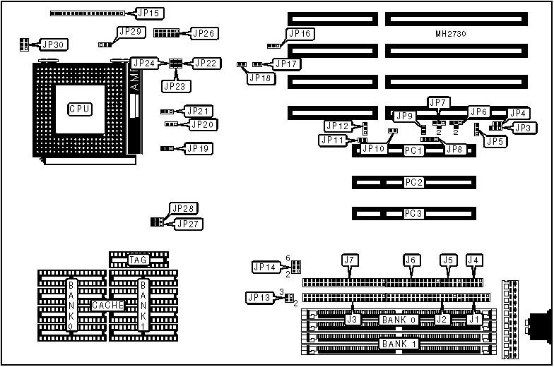
MB-8560/66 AUR
Processor | Pentium |
Processor Speed | 60/66MHz |
Chip Set | Unidentified |
Max. Onboard DRAM | 128MB |
Cache | 256/512/1024KB |
BIOS | Award |
Dimensions | 330mm x 218mm |
I/O Options | 32-bit PCI slots (3), floppy drive interface, IDE interfaces (2), game port, parallel port, serial ports (2) |
NPU Options | None |
CONNECTIONS | |||
Purpose | Location | Purpose | Location |
Game port | J1 | IDE interface LED (secondary) | J13 pins 3 & 4 |
Floppy drive interface | J2 | Speaker | JP15 pins 1 - 4 |
IDE interface (primary) | J3 | Power LED & keylock | JP15 pins 5 - 9 |
Serial port 1 | J4 | Turbo LED | JP15 pins 10 - 11 |
Serial port 2 | J5 | Reset switch | JP15 pins 12 - 13 |
Parallel port | J6 | 5v ground | JP15 pins 17 - 18 |
IDE interface (secondary) | J7 | Chassis fan power | JP30 |
IDE interface LED (primary) | J13 pins 1 & 2 | 32-bit PCI slots | PCI - PC3 |
USER CONFIGURABLE SETTINGS | |||
Function | Jumper | Position | |
» | ECP/EPP mode enabled | JP3 | pins 1 & 2 closed |
SPP mode enabled | JP3 | pins 2 & 3 closed | |
» | CMOS memory normal operation | JP8 | Open |
CMOS memory clear | JP8 | pins 3 & 4 closed | |
Battery type select external | JP8 | Closed | |
» | Factory configured - do not alter | JP9 | Closed |
» | Real time clock type select module type | JP10 | Open |
Real time clock type select normal type | JP10 | Closed | |
» | CMOS memory normal operation | JP11 | Open |
CMOS memory clear | JP11 | Closed | |
» | Factory configured - do not alter | JP12 | pins 2 & 3 closed |
» | Factory configured - do not alter | JP14 | pins 3 & 4, 5 & 6 closed |
» | Flash BIOS voltage select 5v | JP16 | pins 2 & 3 closed |
Flash BIOS voltage select 12v | JP16 | pins 1 & 2 closed | |
» | Factory configured - do not alter | JP17 | N/A |
» | ADS signal select normal | JP18 | Open |
ADS signal select delayed | JP18 | Closed | |
» | CPU ready delay select normal operation | JP19 | pins 2 & 3 closed |
CPU ready delay select CPU delay | JP19 | pins 1 & 2 closed | |
» | Factory configured - do not alter | JP20 | pins 1 & 2 closed |
» | Bridge clock source select from M1449 | JP21 | pins 1 & 2 closed |
Bridge clock source select from clock generator | JP21 | pins 2 & 3 closed | |
» | Factory configured - do not alter | JP26 | N/A |
» | Power good signal detect from power supply | JP29 | pins 1 & 2 closed |
Power good signal detect from board | JP29 | pins 2 & 3 closed | |
DRAM CONFIGURATION | ||
Size | Bank 0 | Bank 1 |
2MB | (2) 256K x 36 | NONE |
4MB | (2) 512K x 36 | NONE |
4MB | (2) 256K x 36 | (2) 256K x 36 |
6MB | (2) 256K x 36 | (2) 512K x 36 |
8MB | (2) 1M x 36 | NONE |
8MB | (2) 512K x 36 | (2) 512K x 36 |
10MB | (2) 256K x 36 | (2) 1M x 36 |
12MB | (2) 512K x 36 | (2) 1M x 36 |
16MB | (2) 2M x 36 | NONE |
16MB | (2) 1M x 36 | (2) 1M x 36 |
18MB | (2) 256K x 36 | (2) 2M x 36 |
20MB | (2) 512K x 36 | (2) 2M x 36 |
24MB | (2) 1M x 36 | (2) 2M x 36 |
32MB | (2) 4M x 36 | NONE |
32MB | (2) 2M x 36 | (2) 2M x 36 |
34MB | (2) 256K x 36 | (2) 4M x 36 |
DRAM CONFIGURATION (CON’T) | ||
Size | Bank 0 | Bank 1 |
36MB | (2) 512K x 36 | (2) 4M x 36 |
40MB | (2) 1M x 36 | (2) 4M x 36 |
48MB | (2) 2M x 36 | (2) 4M x 36 |
64MB | (2) 8M x 36 | NONE |
64MB | (2) 8M x 36 | (2) 4M x 36 |
66MB | (2) 256K x 36 | (2) 8M x 36 |
68MB | (2) 512K x 36 | (2) 8M x 36 |
72MB | (2) 1M x 36 | (2) 8M x 36 |
80MB | (2) 2M x 36 | (2) 8M x 36 |
96MB | (2) 4M x 36 | (2) 8M x 36 |
128MB | (2) 8M x 36 | (2) 8M x 36 |
CACHE CONFIGURATION | |||
Size | Bank 0 | Bank 1 | TAG |
256KB | (4) 32K x 8 | (4) 32K x 8 | (1) 8K x 8 |
512KB | (4) 64K x 8 | (4) 64K x 8 | (1) 16K x 8 |
1MB | (4) 128K x 8 | (4) 128K x 8 | (1) 32K x 8 |
CACHE JUMPER CONFIGURATION | ||
Size | JP27 | JP28 |
256KB | pins 1 & 2 closed | pins 1 & 2 closed |
512KB | pins 2 & 3 closed | pins 1 & 2 closed |
1MB | pins 2 & 3 closed | pins 2 & 3 closed |
CPU SPEED CONFIGURATION | |||
Speed | JP22 | JP23 | JP24 |
60MHz | Open | Closed | Open |
66MHz | Closed | Open | Closed |
DMA CONFIGURATION | ||
DMA | JP6 | JP7 |
DMA1 | pins 1 & 3 closed | pins 1 & 3 closed |
DMA3 | pins 2 & 3 closed | pins 2 & 3 closed |
U2 = 82C863XX | pins 3 & 4 closed | pins 3 & 4 closed |
ECP/EPP/SPP CONFIGURATION | ||
Type | JP4 | JP5 |
U2 = 82C863XX | Open | pins 1 & 3 closed |
U2 = 82C8663XX | Closed | pins 2 & 3 closed |
My Books

