


VL/I-486SV2G, VL/I-486SV2GX4 (REV. 1.1) Motherboard Settings and Configuration
ASUS COMPUTER INTERNATIONAL
VL/I-486SV2G, VL/I-486SV2GX4 (REV. 1.1)
Processor | 80486SX/SL80486SX/80487SX/CX486S/CX486DX/80486DX/SL80486DX/ SLODP486/ODP486SX/CX486DX2/80486DX2/80486DX4/Pentium Overdrive |
Processor Speed | 20/25/33/40/50(internal)/50/66(internal)/75(internal)/82.5(internal)/ 99(internal)/100(internal)MHz |
Chip Set | SIS |
Max. Onboard DRAM | 64MB |
Cache | 128/256/512/1024KB |
BIOS | Award |
Dimensions | 220mm x 220mm |
I/O Options | 32-bit VESA local bus slots (2), PS/2 mouse port, green PC |
NPU Options | None |
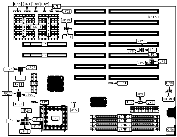
CONNECTIONS | |||
Purpose | Location | Purpose | Location |
External battery | BCON1 | Green PC 1 | JP2 |
Turbo switch | CN1 | Green PC 2 | JP3 |
Turbo LED | CN2 | Green PC 3 | JP4 |
Reset switch | CN3 | Suspend power management | JP28 |
Speaker | CN4 | 32-bit VESA local bus slot | S1 |
Power LED & keylock | CN5 | 32-bit VESA local bus slot | S2 |
PS/2 mouse connector | CN6 |
|
|
USER CONFIGURABLE SETTINGS | |||
Function | Jumper | Position | |
» | Battery type select (Internal) | JP1 | pins 1 & 2 closed |
| Battery type select (External) | JP1 | pins 2 & 3 closed |
» | IRQ12 enabled | JP7 | pins 1 & 2 closed |
| IRQ12 disabled | JP7 | pins 2 & 3 closed |
» | Factory configured - do not alter | JP8 | N/A |
» | Monitor type select CGA | JP9 | pins 2 & 3 closed |
| Monitor type select monochrome or VGA | JP9 | pins 1 & 2 closed |
» | Hardware SMI switch enabled | JP10 | pins 2 & 3 closed |
| RC control enabled | JP10 | pins 1 & 2 closed |
» | CPU manufacturer select type Intel | JP11 | pins 2 & 3 closed |
| CPU manufacturer select type Cyrix | JP11 | pins 1 & 2 closed |
» | Delay VESA clock | JP24 | pins 1 & 2 closed |
| No Delay VESA clock | JP24 | pins 2 & 3 closed |
DRAM CONFIGURATION | ||||
Size | Bank 0 | Bank 1 | Bank 2 | Bank 3 |
1MB | (1) 1M x 36 | NONE | NONE | NONE |
2MB | (1) 1M x 36 | (1) 1M x 36 | NONE | NONE |
2MB | (1) 2M x 36 | NONE | NONE | NONE |
4MB | (1) 4M x 36 | NONE | NONE | NONE |
5MB | (1) 1M x 36 | (1) 4M x 36 | (1) 4M x 36 | NONE |
6MB | (1) 1M x 36 | (1) 1M x 36 | (1) 4M x 36 | (1) 4M x 36 |
6MB | (1) 2M x 36 | NONE | (1) 4M x 36 | NONE |
8MB | (1) 4M x 36 | (1) 4M x 36 | NONE | NONE |
10MB | (1) 1M x 36 | (1) 1M x 36 | (1) 4M x 36 | (1) 4M x 36 |
10MB | (1) 1M x 36 | (1) 1M x 36 | (1) 8M x 36 | NONE |
10MB | (1) 2M x 36 | NONE | (1) 4M x 36 | (1) 4M x 36 |
10MB | (1) 2M x 36 | NONE | (1) 8M x 36 | NONE |
12MB | (1) 4M x 36 | (1) 4M x 36 | (1) 4M x 36 | NONE |
12MB | (1) 8M x 36 | NONE | (1) 4M x 36 | NONE |
16MB | (1) 4M x 36 | (1) 4M x 36 | (1) 4M x 36 | (1) 4M x 36 |
16MB | (1) 4M x 36 | (1) 4M x 36 | (1) 8M x 36 | NONE |
16MB | (1) 8M x 36 | NONE | (1) 8M x 36 | NONE |
16MB | (1) 8M x 36 | NONE | (1) 4M x 36 | (1) 4M x 36 |
16MB | (1) 16M x 36 | NONE | NONE | NONE |
17MB | (1) 1M x 36 | (1) 16M x 36 | NONE | NONE |
18MB | (1) 1M x 36 | (1) 1M x 36 | (1) 16M x 36 | NONE |
18MB | (1) 2M x 36 | NONE | (1) 16M x 36 | NONE |
20MB | (1) 4M x 36 | (1) 16M x 36 | NONE | NONE |
24MB | (1) 4M x 36 | (1) 4M x 36 | (1) 16M x 36 | NONE |
24MB | (1) 8M x 36 | NONE | (1) 16M x 36 | NONE |
32MB | (1) 16M x 36 | (1) 16M x 36 | NONE | NONE |
32MB | (1) 32M x 36 | NONE | NONE | NONE |
36MB | (1) 4M x 36 | (1) 16M x 36 | (1) 16M x 36 | NONE |
DRAM CONFIGURATION (CONT.) | ||||
Size | Bank 0 | Bank 1 | Bank 2 | Bank 3 |
40MB | (1) 4M x 36 | (1) 4M x 36 | (1) 16M x 36 | (1) 16M x 36 |
40MB | (1) 4M x 36 | (1) 4M x 36 | (1) 32M x 36 | NONE |
40MB | (1) 8M x 36 | NONE | (1) 16M x 36 | (1) 16M x 36 |
40MB | (1) 8M x 36 | NONE | (1) 32M x 36 | NONE |
40MB | (1) 16M x 36 | (1) 16M x 36 | (1) 16M x 36 | NONE |
64MB | (1) 16M x 36 | (1) 16M x 36 | (1) 16M x 36 | (1) 16M x 36 |
64MB | (1) 16M x 36 | (1) 16M x 36 | (1) 32M x 36 | NONE |
64MB | (1) 32M x 36 | NONE | (1) 32M x 36 | NONE |
CACHE CONFIGURATION | |||
Size | Bank 0 | Bank 1 | TAG |
128KB | (4) 32K x 8 | NONE | (1) 8K x 8 |
256KB | (4) 32K x 8/(4) 64K x 8 | (4) 32K x 8/NONE | (1) 32K x 8 |
512KB | (4) 64K x 8/(4) 128K x 8 | (4) 64K x 8/NONE | (1) 32K x 8 |
1024KB | (4) 128K x 8 | (4) 128K x 8 | (1) 128K x 8 |
CACHE JUMPER CONFIGURATION | |||
Size | JP13 | JP14 | JP25 |
128KB | Open | pins 2 & 3 closed | pins 1 & 2 closed |
256KB (32K x 8) | Open | pins 1 & 2 closed | pins 1 & 2 closed |
256KB (64K x 8) | pins 1 & 2 closed | pins 2 & 3 closed | pins 1 & 2 closed |
512KB (64K x 8) | pins 5 & 6 closed | pins 1 & 2 closed | pins 2 & 3 closed |
512KB (128K x 8) | pins 1 & 2 closed | pins 2 & 3 closed | pins 2 & 3 closed |
1024KB | pins 2 & 3 closed | pins 1 & 2 closed | pins 2 & 3 closed |
CPU TYPE CONFIGURATION | |||||
Type | JP16 | JP17 | JP18 | JP19 | JP20 |
80486SX | Open | Open | Open | pins 2 & 3 | pins 2 & 3 |
SL486SX | 3 & 4 and 5 & 6 | Open | pins 4 & 5 | pins 2 & 3 | pins 2 & 3 |
80487SX | Open | Open | Open | pins 1 & 2 | pins 2 & 3 |
CX486S | 2 & 3 and 4 & 5 | pins 1 & 2 | 1 & 2 and 3 & 4 | pins 2 & 3 | pins 2 & 3 |
CX486DX | 2 & 3 and 4 & 5 | pins 1 & 2 | 1 & 2 and 3 & 4 | pins 1 & 2 | pins 2 & 3 |
80486DX | Open | Open | Open | pins 1 & 2 | pins 2 & 3 |
SL486DX | 3 & 4 and 5 & 6 | Open | pins 4 & 5 | pins 1 & 2 | pins 2 & 3 |
SLODP486 | pins 5 & 6 | Open | pins 4 & 5 | pins 1 & 2 | pins 2 & 3 |
ODP486SX | Open | Open | Open | pins 1 & 2 | pins 2 & 3 |
CX486DX2 | 2 & 3 and 4 & 5 | pins 1 & 2 | 1 & 2 and 3 & 4 | 1 & 2 and 4 & 5 | pins 2 & 3 |
80486DX2 | Open | Open | Open | pins 1 & 2 | pins 2 & 3 |
SL486DX2 | 3 & 4 and 5 & 6 | Open | pins 4 & 5 | pins 1 & 2 | pins 2 & 3 |
80486DX4 (2 x) | 3 & 4 and 5 & 6 | pins 5 & 6 | pins 4 & 5 | pins 1 & 2 | pins 2 & 3 |
80486DX4 (2.5 x) | 3 & 4 and 5 & 6 | pins 4 & 5 | pins 4 & 5 | pins 1 & 2 | pins 2 & 3 |
80486DX4 (3 x) | 3 & 4 and 5 & 6 | Open | pins 4 & 5 | pins 1 & 2 | pins 2 & 3 |
Pentium Overdrive | pins 5 & 6 | Open | pins 4 & 5 | pins 1 & 2 | pins 1 & 2 |
Note:Pins designated should be in the closed position. | |||||
HARDWARE TRAP CPU TYPE CONFIGURATION | ||
Type | JP5 | JP6 |
80486SX | pins 1 & 2 closed | pins 2 & 3 closed |
CX486S | pins 2 & 3 closed | pins 1 & 2 closed |
CX486DX | pins 2 & 3 closed | pins 1 & 2 closed |
80486DX | pins 1 & 2 closed | pins 2 & 3 closed |
SL486SX | pins 1 & 2 closed | pins 2 & 3 closed |
SL486DX | pins 1 & 2 closed | pins 2 & 3 closed |
80486DX2 | pins 1 & 2 closed | pins 2 & 3 closed |
SL486DX2 | pins 1 & 2 closed | pins 2 & 3 closed |
SL486DX4 | pins 1 & 2 closed | pins 2 & 3 closed |
Pentium Overdrive | pins 1 & 2 closed | pins 1 & 2 closed |
CPU SPEED CONFIGURATION | |||
Speed | JP21 | JP22 | JP23 |
20MHz | pins 1 & 2 closed | pins 1 & 2 closed | pins 1 & 2 closed |
25MHz | pins 2 & 3 closed | pins 1 & 2 closed | pins 1 & 2 closed |
33MHz | pins 2 & 3 closed | pins 2 & 3 closed | pins 2 & 3 closed |
40MHz | pins 2 & 3 closed | pins 2 & 3 closed | pins 1 & 2 closed |
50i MHz | pins 2 & 3 closed | pins 1 & 2 closed | pins 1 & 2 closed |
50MHz | pins 1 & 2 closed | pins 1 & 2 closed | pins 2 & 3 closed |
66i MHz | pins 2 & 3 closed | pins 2 & 3 closed | pins 2 & 3 closed |
75i MHz (3x) | pins 2 & 3 closed | pins 1 & 2 closed | pins 1 & 2 closed |
82.5i MHz (2.5x) | pins 2 & 3 closed | pins 2 & 3 closed | pins 2 & 3 closed |
99i MHz (3x) | pins 2 & 3 closed | pins 2 & 3 closed | pins 2 & 3 closed |
100i MHz (2x) | pins 1 & 2 closed | pins 1 & 2 closed | pins 2 & 3 closed |
VESA WAIT STATE/BUS SPEED CONFIGURATION | |||
CPU speed | Wait states | JP26 | JP27 |
<=33MHz | 0 wait states | pins 1 & 2 closed | pins 1 & 2 closed |
>33MHz | 1 wait state | pins 2 & 3 closed | pins 2 & 3 closed |
CPU VOLTAGE SELECTION | ||
Function | JP12 | JP15 |
3.3V (DX4) | pins 2 & 3 closed | pins 2 & 3 closed |
5V | pins 1 & 2 closed | pins 1 & 2 closed |


My Books

