MCT-VIO Hard Disk/Floppy Controller Settings and Configuration
MODULAR CIRCUIT TECHNOLOGY
MCT-VIO
Data bus: | 32-bit, VL-bus |
Size: | Three/quarter-length, full-height card |
Hard drive supported: | Two IDE (AT) interface drives |
Floppy drives supported: | Two 360KB, 720KB, 1.2MB, or 1.44MB drives |
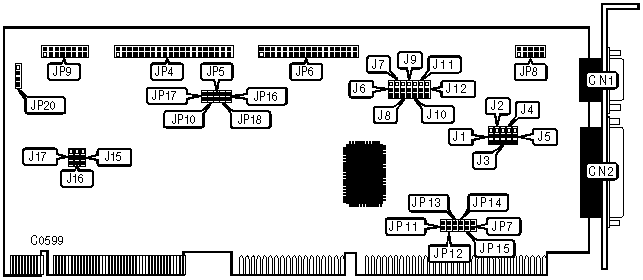
CONNECTIONS | |
Function | Location |
9-pin serial port - external | CN1 |
25-pin parallel port - external | CN2 |
40-pin IDE (AT) Interface connector | JP4 |
34-pin control cable connector - floppy drive | JP6 |
10-pin serial port - internal | JP8 |
16-pin game port - internal | JP9 |
4-pin connector - drive active LED | JP20 |
USER CONFIGURABLE SETTINGS | |||
Function | Location | Setting | |
| » | Floppy drive enable | J1 | pins 2 & 3 closed |
| » | Floppy drive disable | J1 | pins 1 & 2 closed |
| » | IDE address is 1F0-1F7 | J2 | pins 2 & 3 closed |
| » | IDE address is 170-177 | J2 | pins 1 & 2 closed |
| » | Floppy drive designation normal | J3 | pins 2 & 3 closed |
| » | Floppy drive designation change | J3 | pins 1 & 2 closed |
| » | IDE controller enable | J4 | pins 2 & 3 closed |
| » | IDE controller disable | J4 | pins 1 & 2 closed |
| » | IDE I/O address is 1F0-1F7, 3F0-3F7 | J5 | pins 2 & 3 closed |
| » | IDE I/O address is 170-177, 370-377 | J5 | pins 1 & 2 closed |
| » | Game port enable | J12 | pins 2 & 3 closed |
| » | Game port disable | J12 | Pins 1 & 2 closed |
| » | 1 IDE drive installed | JP5 | closed |
| » | 2 IDE drives installed (master/slave) | JP5 | open |
| » | Printer port as bi-directional | JP7 | closed |
| » | Printer port as uni-directional | JP7 | open |
| » | IDE(AT) interrupt select IRQ 14 | JP10 | closed |
| » | IRQ 14 disabled | JP10 | open |
| » | COM2 or COM4 interrupt select IRQ 3 | JP11 | closed |
| » | IRQ 3 disabled | JP11 | open |
| » | COM1 or COM3 interrupt select IRQ 4 | JP12 | closed |
| » | IRQ 4 disabled | JP12 | open |
| » | FDC interrupt select IRQ 6 | JP13 | closed |
| » | IRQ 6 disabled | JP13 | open |
| » | IRQ 5 disabled | JP14 | open |
| » | LPT interrupt select IRQ 5 | JP14 | closed |
| » | LPT interrupt select IRQ 7 | JP15 | closed |
| » | IRQ 7 disabled | JP15 | open |
| » | Factory configured - do not alter | JP16 | N/A |
| » | Factory configured - do not alter | JP18 | N/A |
PARALLEL PORT CONFIGURATION | |||
LPT | J6 | J7 | |
| » | LPT1 (378-37F) | pins 2 & 3 closed | pins 2 & 3 closed |
| » | LPT2 (278-27F) | pins 1 & 2 closed | pins 1 & 2 closed |
| » | LPT3 (3BC-3BE) | pins 2 & 3 closed | pins 1 & 2 closed |
| » | Disabled | pins 1 & 2 closed | pins 2 & 3 closed |
SERIAL PORT 1 CONFIGURATION | |||
COM | J8 | J9 | |
| » | COM1 (3F8-3FF) | pins 2 & 3 closed | pins 2 & 3 closed |
| » | COM3 (3E8-3EF) | pins 1 & 2 closed | pins 1 & 2 closed |
| » | COM4 (2E8-2EF) | pins 2 & 3 closed | pins 1 & 2 closed |
| » | Disabled | pins 1 & 2 closed | pins 2 & 3 closed |
SERIAL PORT 2 CONFIGURATION | |||
COM | J10 | J11 | |
| » | COM2 (2F8-2FF) | pins 2 & 3 closed | pins 2 & 3 closed |
| » | COM4 (2E8-2EF) | pins 1 & 2 closed | pins 1 & 2 closed |
| » | COM3 (3E8-3EF) | pins 2 & 3 closed | pins 1 & 2 closed |
| » | Disable | pins 1 & 2 closed | pins 2 & 3 closed |
VESA /ISA CONFIGURATION | |||
Mode | J15 | JP17 | |
| » | VESA | pins 2 & 3 closed | open |
| » | ISA | pins 1 & 2 closed | closed |
IDE WAIT STATE CONTROL | |||
IDE Wait State Control | J16 | J17 | |
| » | 50MHz VL bus clock | pins 2 & 3 closed | pins 2 & 3 closed |
| » | 25MHz VL bus clock | pins 1 & 2 closed | pins 1 & 2 closed |
| » | 33MHz VL bus clock | pins 2 & 3 closed | pins 1 & 2 closed |
| » | 40MHz VL bus clock | pins 1 & 2 closed | pins 2 & 3 closed |
MISCELLANEOUS TECHNICAL NOTES |
50MHz is not part of the VESA standard and may not be compatible with some systems. |
My Books

