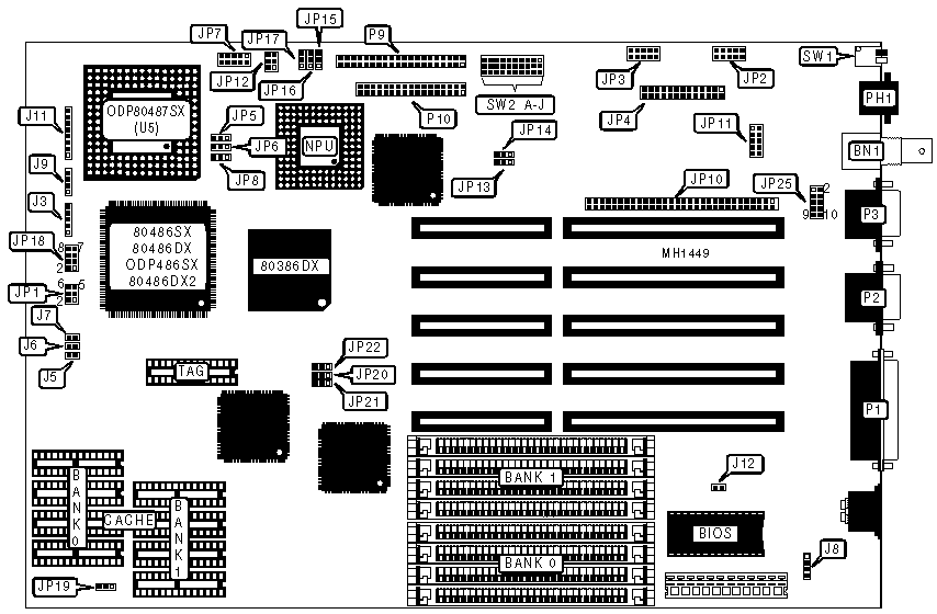
XI-386/486/386SX Motherboard Settings and Configuration
XINETRON, INC.
XI-386/486/386SX
Processor | 80386DX/80486SX/80487SX/80486DX/ODP486SX/80486DX2 |
Processor Speed | 20/25/33/50(Internal)/50/66(Internal)MHz |
Chip Set | Xinetron |
Max. onboard DRAM | 32MB |
Cache | 64/128/256KB |
BIOS | AMI |
Dimensions | 330mm x 218mm |
I/O Options | Ethernet (2), Floppy drive interface, IDE interface, parallel port, serial port (2) |
NPU Options | 80387DX/3167 |
CONNECTIONS | |||
Purpose | Location | Purpose | Location |
Ethernet BNC | BN1 | Hercules graphic signal output | JP7 |
Power LED & keylock | J3 | LAN board connector | JP10 |
Turbo LED | J5 | LAN board connector | JP11 |
Turbo switch | J6 | Parallel port | P1 |
Reset switch | J7 | Serial port 1 | P2 |
External battery | J8 | Serial port 1 | P3 |
Speaker | J9 | IDE interface | P9 |
Serial port 1 | JP2 | Floppy drive interface | P10 |
Serial port 1 | JP3 | Ethernet twisted pair | PH1 |
Parallel port | JP4 |
|
|
. USER CONFIGURABLE SETTINGS | |||
Function | Jumper/Switch | Position | |
» | Factory configured - do not alter | J11 | Closed |
» | Monitor type select color | J12 | pins 1 & 2 open |
| Monitor type select monochrome | J12 | pins 1 & 2 closed |
» | AT BUS clock select synchronous | JP1 | pins 5 & 6 closed |
| AT BUS clock select asynchronous | JP1 | pins 4 & 5 closed |
» | Hercules Graphic display enabled | JP5 & JP6 | pins 1 & 2 closed |
| Hercules Graphic display disabled | JP5 & JP6 | pins 2 & 3 closed |
» | Hercules Graphic display select character generator enable | JP8 | pins 1 & 2 closed |
| Hercules Graphic display select character generator disabled | JP8 | pins 2 & 3 closed |
» | NPU select 3167 or 387DX enabled | JP12 | pins 4 & 5 closed |
| NPU select 3167 or 387DX disabled | JP12 | pins 5 & 6 closed |
» | I/O ports enabled addresses set to primary | JP25 | pins 1 & 2 closed |
» | Factory configured - do not alter | SW1/switch 1 | Off |
» | Ethernet type select 10BaseT | SW1/switch 2 | On |
| Ethernet type select 10Base2 | SW1/switch 2 | Off |
» | Serial port COM1 I/O address select 3e8h | SW2A | pins 2 & 3 closed |
| Serial port COM1 I/O address select 3f8h | SW2B | pins 1 & 2 closed |
» | Serial port COM2 I/O address select 2e8h | SW2C | pins 2 & 3 closed |
| Serial port COM2 I/O address select 2f8h | SW2D | pins 1 & 2 closed |
» | Parallel port I/O address select 278h | SW2E | pins 2 & 3 closed |
| Parallel port I/O address select 378h | SW2F | pins 1 & 2 closed |
» | Floppy drive controller select primary | SW2G | pins 2 & 3 closed |
| Floppy drive controller select secondary | SW2H | pins 1 & 2 closed |
» | IDE interface select primary | SW2I | pins 2 & 3 closed |
| IDE interface select secondary | SW2J | pins 1 & 2 closed |
CPU TYPE CONFIGURATION | |||||
CPU | Type | JP1 | JP20 - JP22 | JP13 - JP17 | U49 |
80386DX | PGA | N/A | pins 2 & 3 | pins 2 & 3 | 386 BIOS |
80486SX | PQFP | pins 1 & 2 | pins 1 & 2 | pins 2 & 3 | 486 BIOS |
80486DX | PQFP | pins 2 & 3 | pins 1 & 2 | pins 2 & 3 | 486 BIOS |
ODP486SX | P23T (U5) | pins 2 & 3 | pins 1 & 2 | pins 1 & 2 | 486 BIOS |
80486DX2 | P23T (U5) | pins 2 & 3 | pins 1 & 2 | pins 1 & 2 | 486 BIOS |
Note:Pins designated should be in the closed position. | |||||
DRAM CONFIGURATION | ||
Size | Bank 0 | Bank 1 |
1MB | (4) 256K x 9 | NONE |
2MB | (4) 256K x 9 | (4) 256K x 9 |
4MB | (4) 1M x 9 | NONE |
5MB | (4) 256K x 9 | (4) 1M x 9 |
8MB | (4) 1M x 9 | (4) 1M x 9 |
16MB | (4) 4M x 9 | NONE |
20MB | (4) 1M x 9 | (4) 4M x 9 |
32MB | (4) 4M x 9 | (4) 4M x 9 |
CACHE JUMPER CONFIGURATION | ||
Size | JP18 | JP19 |
64KB | pins 1 & 2, 4 & 5, 6 & 7 closed | pins 1 & 2 closed |
128KB | pins 2 & 3, 5 & 6 closed | pins 2 & 3 closed |
256KB | pins 2 & 3, 5 & 6 closed | pins 2 & 3 closed |
CACHE CONFIGURATION | |||
Size | Bank 0 | Location | TAG |
64KB | (4) 8K x 8 | (4) 8K x 8 | (1) 8K x 8 |
128KB | (4) 32K x 8 | NONE | (1) 8K x 8 |
256KB | (4) 32K x 8 | (4) 32K x 8 | (1) 32K x 8 |
My Books

